The conductivity of an intrinsic semiconductor depends on its temperature, but at room temperature its conductivity is very low. As such, no important electronic devices can be developed using these semiconductors. Hence there is a necessity of improving their conductivity. This can be done by making use of impurities.
When a small amount, say, a few parts per million (ppm), of a suitable impurity is added to the pure semiconductor, the conductivity of the semiconductor is increased manifold. Such materials are known as extrinsic semiconductors or impurity semiconductors. The deliberate addition of a desirable impurity is called doping and the impurity atoms are called dopants. Such a material is also called a doped semiconductor. The dopant has to be such that it does not distort the original pure semiconductor lattice. It occupies only a very few of the original semiconductor atom sites in the crystal. A necessary condition to attain this is that the sizes of the dopant and the semiconductor atoms should be nearly the same.
There are two types of dopants used in doping the tetravalent Si or Ge:
(i) Pentavalent (valency 5); like Arsenic (As), Antimony (Sb), Phosphorous (P), etc.
(ii) Trivalent (valency 3); like Indium (In), Boron (B), Aluminium (Al), etc.
We shall now discuss how the doping changes the number of charge carriers (and hence the conductivity) of semiconductors. Si or Ge belongs to the fourth group in the Periodic table and, therefore, we choose the dopant element from nearby fifth or third group, expecting and taking care that the size of the dopant atom is nearly the same as that of Si or Ge. Interestingly, the pentavalent and trivalent dopants in Si or Ge give two entirely different types of semiconductors as discussed below.
(i) n-type semiconductor
Suppose we dope Si or Ge with a pentavalent element as shown in Fig. 14.7. When an atom of +5 valency element occupies the position of an atom in the crystal lattice of Si, four of its electrons bond with the four silicon neighbours while the fifth remains very weakly bound to its parent atom. This is because the four electrons participating in bonding are seen as part of the effective core of the atom by the fifth electron. As a result the ionisation energy required to set this electron free is very small and even at room temperature it will be free to move in the lattice of the semiconductor. For example, the energy required is ~ 0.01 eV for germanium, and 0.05 eV for silicon, to separate this electron from its atom. This is in contrast to the energy required to jump the forbidden band (about 0.72 eV for germanium and about 1.1 eV for silicon) at room temperature in the intrinsic semiconductor. Thus, the pentavalent dopant is donating one extra electron for conduction and hence is known as donor impurity. The number of electrons made available for conduction by dopant atoms depends strongly upon the doping level and is independent of any increase in ambient temperature. On the other hand, the number of free electrons (with an equal number of holes) generated by Si atoms, increases weakly with temperature.
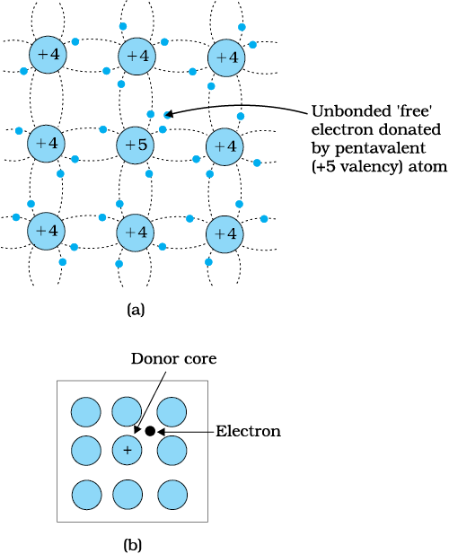
Figure 14.7 (a) Pentavalent donor atom (As, Sb, P, etc.) doped for tetravalent Si or Ge giving n-type semiconductor, and (b) Commonly used schematic representation of n-type material which shows only the fixed cores of the substituent donors with one additional effective positive charge and its associated extra electron.
In a doped semiconductor the total number of conduction electrons ne is due to the electrons contributed by donors and those generated intrinsically, while the total number of holes nh is only due to the holes from the intrinsic source. But the rate of recombination of holes would increase due to the increase in the number of electrons. As a result, the number of holes would get reduced further.
Thus, with proper level of doping the number of conduction electrons can be made much larger than the number of holes. Hence in an extrinsic semiconductor doped with pentavalent impurity, electrons become the majority carriers and holes the minority carriers. These semiconductors are, therefore, known as n-type semiconductors. For n-type semiconductors, we have,
ne >> nh (14.3)
(ii) p-type semiconductor
This is obtained when Si or Ge is doped with a trivalent impurity like Al, B, In, etc. The dopant has one valence electron less than Si or Ge and, therefore, this atom can form covalent bonds with neighbouring three Si atoms but does not have any electron to offer to the fourth Si atom. So the bond between the fourth neighbour and the trivalent atom has a vacancy or hole as shown in Fig. 14.8. Since the neighbouring Si atom in the lattice wants an electron in place of a hole, an electron in the outer orbit of an atom in the neighbourhood may jump to fill this vacancy, leaving a vacancy or hole at its own site. Thus the hole is available for conduction. Note that the trivalent foreign atom becomes effectively negatively charged when it shares fourth electron with neighbouring Si atom. Therefore, the dopant atom of p-type material can be treated as core of one negative charge along with its associated hole as shown in Fig. 14.8(b). It is obvious that one acceptor atom gives one hole. These holes are in addition to the intrinsically generated holes while the source of conduction electrons is only intrinsic generation. Thus, for such a material, the holes are the majority carriers and electrons are minority carriers. Therefore, extrinsic semiconductors doped with trivalent impurity are called p-type semiconductors. For p-type semiconductors, the recombination process will reduce the number (ni)of intrinsically generated electrons to ne. We have, for p-type semiconductors
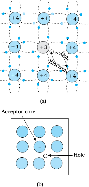
Figure 14.8 (a) Trivalent acceptor atom (In, Al, B etc.) doped in tetravalent Si or Ge lattice giving p-type semiconductor. (b) Commonly used schematic representation of p-type material which shows only the fixed core of the substituent acceptor with one effective additional negative charge and its associated hole.
nh >> ne (14.4)
Note that the crystal maintains an overall charge neutrality as the charge of additional charge carriers is just equal and opposite to that of the ionised cores in the lattice.
In extrinsic semiconductors, because of the abundance of majority current carriers, the minority carriers produced thermally have more chance of meeting majority carriers and thus getting destroyed. Hence, the dopant, by adding a large number of current carriers of one type, which become the majority carriers, indirectly helps to reduce the intrinsic concentration of minority carriers.
The semiconductor’s energy band structure is affected by doping. In the case of extrinsic semiconductors, additional energy states due to donor impurities (ED) and acceptor impurities (EA) also exist. In the energy band diagram of n-type Si semiconductor, the donor energy level ED is slightly below the bottom EC of the conduction band and electrons from this level move into the conduction band with very small supply of energy. At room temperature, most of the donor atoms get ionised but very few (~10–12) atoms of Si get ionised. So the conduction band will have most electrons coming from the donor impurities, as shown in Fig. 14.9(a). Similarly, for p-type semiconductor, the acceptor energy level EA is slightly above the top EV of the valence band as shown in Fig. 14.9(b). With very small supply of energy an electron from the valence band can jump to the level EA and ionise the acceptor negatively. (Alternately, we can also say that with very small supply of energy the hole from level EA sinks down into the valence band. Electrons rise up and holes fall down when they gain external energy.) At room temperature, most of the acceptor atoms get ionised leaving holes in the valence band. Thus at room temperature the density of holes in the valence band is predominantly due to impurity in the extrinsic semiconductor. The electron and hole concentration in a semiconductor in thermal equilibrium is given by
nenh = ni2 (14.5)
Though the above description is grossly approximate and hypothetical, it helps in understanding the difference between metals, insulators and semiconductors (extrinsic and intrinsic) in a simple manner. The difference in the resistivity of C, Si and Ge depends upon the energy gap between their conduction and valence bands. For C (diamond), Si and Ge, the energy gaps are 5.4 eV, 1.1 eV and 0.7 eV, respectively. Sn also is a group IV element but it is a metal because the energy gap in its case is 0 eV.
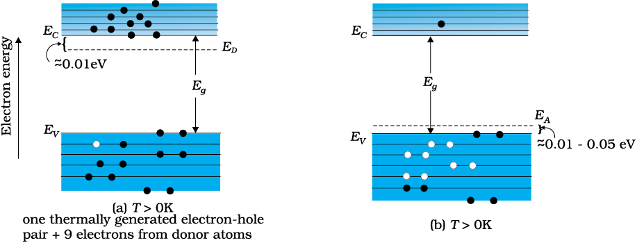
Figure 14.9 Energy bands of (a) n-type semiconductor at T > 0K, (b) p-type
semiconductor at T > 0K.
Example 14.2 Suppose a pure Si crystal has 5 × 1028 atoms m–3. It is doped by 1 ppm concentration of pentavalent As. Calculate the number of electrons and holes. Given that ni =1.5 × 10¹⁶ m–3.
Solution Note that thermally generated electrons (ni ~1016 m–3) are negligibly small as compared to those produced by doping.
Therefore, ne ≈ ND.
Since nenh = ni2, The number of holes
nh = (2.25 × 1032)/(5 ×1022)
~ 4.5 × 10⁹ m–3
© 2026 GoodEd Technologies Pvt. Ltd.

