We have seen so far, how a semiconductor diode behaves under applied electrical inputs. In this section, we learn about semiconductor diodes in which carriers are generated by photons (photo-excitation). All these devices are called optoelectronic devices. We shall study the functioning of the following optoelectronic devices:
(i) Photodiodes used for detecting optical signal (photodetectors).
(ii) Light emitting diodes (LED) which convert electrical energy into light.
(iii) Photovoltaic devices which convert optical radiation into electricity (solar cells).
(i) Photodiode
A Photodiode is again a special purpose p-n junction diode fabricated with a transparent window to allow light to fall on the diode. It is operated under reverse bias. When the photodiode is illuminated with light (photons) with energy (hν) greater than the energy gap (Eg) of the semiconductor, then electron-hole pairs are generated due to the absorption of photons. The diode is fabricated such that the generation of e-h pairs takes place in or near the depletion region of the diode. Due to electric field of the junction, electrons and holes are separated before they recombine. The direction of the electric field is such that electrons reach n-side and holes reach p-side. Electrons are collected on n-side and holes are collected on p-side giving rise to an emf. When an external load is connected, current flows. The magnitude of the photocurrent depends on the intensity of incident light (photocurrent is proportional to incident light intensity).
It is easier to observe the change in the current with change in the light intensity, if a reverse bias is applied. Thus photodiode can be used as a photodetector to detect optical signals. The circuit diagram used for the measurement of I-V characteristics of a photodiode is shown in Fig. 14.23(a) and a typical I-V characteristics in Fig. 14.23(b).
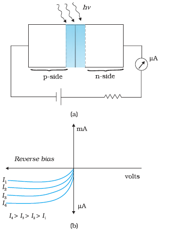
Figure 14.23 (a) An illuminated photodiode under reverse bias , (b) I-V characteristics of a photodiode for different illumination intensity I4 > I3 > I2 > I1.
Example 14.6 The current in the forward bias is known to be more (~mA) than the current in the reverse bias (~µA). What is the reason then to operate the photodiodes in reverse bias?
Solution Consider the case of an n-type semiconductor. Obviously, the majority carrier density (n) is considerably larger than the minority hole density p (i.e., n >> p). On illumination, let the excess electrons and holes generated be ∆n and ∆p, respectively:
n′ = n + ∆n
p′ = p + ∆p
Here n′ and p′ are the electron and hole concentrations* at any particular illumination and n and p are carriers concentration when there is no illumination. Remember ∆n = ∆p and n >> p. Hence, the fractional change in the majority carriers (i.e., ∆n/n) would be much less than that in the minority carriers (i.e., ∆p/p). In general, we can state that the fractional change due to the photo-effects on the minority carrier dominated reverse bias current is more easily measurable than the fractional change in the forward bias current. Hence, photodiodes are preferably used in the reverse bias condition for measuring light intensity.
(ii) Light emitting diode
It is a heavily doped p-n junction which under forward bias emits spontaneous radiation. The diode is encapsulated with a transparent cover so that emitted light can come out.
When the diode is forward biased, electrons are sent from n → p (where they are minority carriers) and holes are sent from p → n (where they are minority carriers). At the junction boundary the concentration of minority carriers increases compared to the equilibrium concentration (i.e., when there is no bias). Thus at the junction boundary on either side of the junction, excess minority carriers are there which recombine with majority carriers near the junction. On recombination, the energy is released in the form of photons. Photons with energy equal to or slightly less than the band gap are emitted. When the forward current of the diode is small, the intensity of light emitted is small. As the forward current increases, intensity of light increases and reaches a maximum. Further increase in the forward current results in decrease of light intensity. LEDs are biased such that the light emitting efficiency is maximum.
The V-I characteristics of a LED is similar to that of a Si junction diode. But the threshold voltages are much higher and slightly different for each colour. The reverse breakdown voltages of LEDs are very low, typically around 5V. So care should be taken that high reverse voltages do not appear across them.
LEDs that can emit red, yellow, orange, green and blue light are commercially available. The semiconductor used for fabrication of visible LEDs must at least have a band gap of 1.8 eV (spectral range of visible light is from about 0.4 µm to 0.7 µm, i.e., from about 3 eV to 1.8 eV). The compound semiconductor Gallium Arsenide – Phosphide (GaAs1–xPx) is used for making LEDs of different colours. GaAs0.6 P0.4 (Eg ~ 1.9 eV) is used for red LED. GaAs (Eg ~ 1.4 eV) is used for making infrared LED. These LEDs find extensive use in remote controls, burglar alarm systems, optical communication, etc. Extensive research is being done for developing white LEDs which can replace incandescent lamps.
LEDs have the following advantages over conventional incandescent low power lamps:
(i) Low operational voltage and less power.
(ii) Fast action and no warm-up time required.
(iii) The bandwidth of emitted light is 100 Å to 500 Å or in other words it is nearly (but not exactly) monochromatic.
(iv) Long life and ruggedness.
(v) Fast on-off switching capability.
(iii) Solar cell
A solar cell is basically a p-n junction which generates emf when solar radiation falls on the p-n junction. It works on the same principle (photovoltaic effect) as the photodiode, except that no external bias is applied and the junction area is kept much larger for solar radiation to be incident because we are interested in more power.
A simple p-n junction solar cell is shown in Fig. 14.24.
A p-Si wafer of about 300 µm is taken over which a thin layer (~0.3 µm) of n-Si is grown on one-side by diffusion process. The other side of p-Si is coated with a metal (back contact). On the top of n-Si layer, metal finger electrode (or metallic grid) is deposited. This acts as a front contact. The metallic grid occupies only a very small fraction of the cell area (<15%) so that light can be incident on the cell from the top.
The generation of emf by a solar cell, when light falls on, it is due to the following three basic processes: generation, separation and collection— (i) generation of e-h pairs due to light (with hν > Eg) close to the junction; (ii) separation of electrons and holes due to electric field of the depletion region. Electrons are swept to n-side and holes to p-side;
(iii) the electrons reaching the n-side are collected by the front contact and holes reaching p-side are collected by the back contact. Thus p-side becomes positive and n-side becomes negative giving rise to photovoltage.
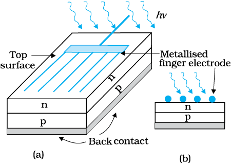
Figure 14.24 (a) Typical p-n junction solar cell; (b) Cross-sectional view.
When an external load is connected as shown in the Fig. 14.25(a) a photocurrent IL flows through the load. A typical I-V characteristics of a solar cell is shown in the Fig. 14.25(b).
Note that the I – V characteristics of solar cell is drawn in the fourth quadrant of the coordinate axes. This is because a solar cell does not draw current but supplies the same to the load.
Semiconductors with band gap close to 1.5 eV are ideal materials for solar cell fabrication. Solar cells are made with semiconductors like Si (Eg = 1.1 eV), GaAs (Eg = 1.43 eV), CdTe (Eg = 1.45 eV), CuInSe2 (Eg = 1.04 eV), etc. The important criteria for the selection of a material for solar cell fabrication are (i) band gap (~1.0 to 1.8 eV), (ii) high optical absorption (~104 cm–1), (iii) electrical conductivity, (iv) availability of the raw material, and (v) cost. Note that sunlight is not always required for a solar cell. Any light with photon energies greater than the bandgap will do. Solar cells are used to power electronic devices in satellites and space vehicles and also as power supply to some calculators. Production of low-cost photovoltaic cells for large-scale solar energy is a topic for research.
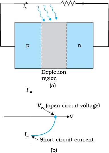
Figure 14.25 (a) A typical illuminated p-n junction solar cell;
(b) I-V characteristics of a solar cell.
Example 14.7 Why are Si and GaAs are preferred materials for solar cells?
Solution The solar radiation spectrum received by us is shown in Fig. 14.26.
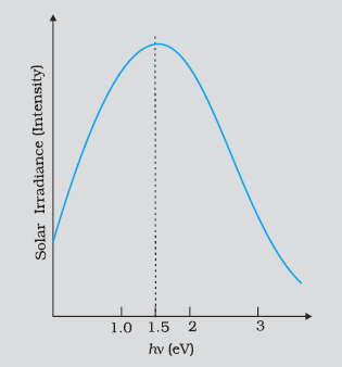
Figure 14.26
The maxima is near 1.5 eV. For photo-excitation, hν > Eg. Hence, semiconductor with band gap ~1.5 eV or lower is likely to give better solar conversion efficiency. Silicon has Eg ~ 1.1 eV while for GaAs it is ~1.53 eV. In fact, GaAs is better (in spite of its higher band gap) than Si because of its relatively higher absorption coefficient. If we choose materials like CdS or CdSe (Eg ~ 2.4 eV), we can use only the high energy component of the solar energy for photo-conversion and a significant part of energy will be of no use.
The question arises: why we do not use material like PbS (Eg ~ 0.4 eV) which satisfy the condition hν > Egfor ν maxima corresponding to the solar radiation spectra? If we do so, most of the solar radiation will be absorbed on the top-layer of solar cell and will not reach in or near the depletion region. For effective electron-hole separation, due to the junction field, we want the photo-generation to occur in the junction region only.
© 2026 GoodEd Technologies Pvt. Ltd.

