
 Q. No.
The circuit shown below is an electrical analogue for which of the following logic gates?

1. AND gate
2. OR gate
3. NOT gate
4. NOR gate
1. AND gate
2. OR gate
3. NOT gate
4. NOR gate


What is the equivalent resistance across the terminals of the battery if the diodes are ideal?
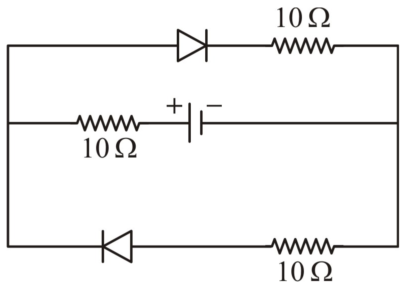
| 1. | \(10~ \Omega\) | 2. | \(20~ \Omega\) |
| 3. | \(15~ \Omega\) | 4. | \({10\over3} ~ \Omega\) |
What is the name of the logic gate represented by the following symbol?

1. NOR
2. OR
3. NAND
4. AND


For the logic circuit given below, the output \(Y\) for \(A=0,B=0\) and \(A=1,B=1\) are:

1. \(0\) and \(1\)
2. \(0\) and \(0\)
3. \(1\) and \(0\)
4. \(1\) and \(1\)
| 1. | becomes four times the initial value. |
| 2. | becomes one-fourth of the initial value. |
| 3. | remains unchanged. |
| 4. | becomes half of the initial value. |
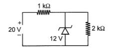
A Zener diode is used to obtain a constant voltage. If applied voltage \(\text V\) changes, then:
(\(\text V\) is more than Zener voltage)

| 1. | \(i_{1}\) and \(i_{2}\) change. |
| 2. | \(i_{2}\) and \(\text V_{0}\) change and \(i_{3}\) remains constant. |
| 3. | \(i_{2}\) and \(\text V_{0}\) don't change while \(i_{3}\) changes. |
| 4. | \(i_{3}\) and \(\text V_{0}\) don't change while \(i_{2}\) changes. |


Which of the following-junction is used unbiased?
1. Photo diode
2. LED
3. Zener diode
4. Solar cell
1. \(36~\text{mW}\)
2. \(12~\text{mW}\)
3. \(144~\text{mW}\)
4. \(72~\text{mW}\)
© 2024 GoodEd Technologies Pvt. Ltd.