
 Q. No.
In the energy band diagram of a material shown below, the open circles and filled circles denote holes and electrons respectively. The material is a/an:

1.
p-type semiconductor
2.
insulator
3.
metal
4.
n-type semiconductor


The given circuit has two ideal diodes connected as shown in the figure below. The current flowing through the resistance R1 will be:

| 1. | 2.5 A | 2. | 10.0 A |
| 3. | 1.43 A | 4. | 3.13 A |
A forward-biased diode is treated as:
| 1. | an open switch with infinite resistance. |
| 2. | a closed switch with a voltage drop of 0 V. |
| 3. | a closed switch in series with a battery with voltage of 0.7 V. |
| 4. | a closed switch in series with small resistance and a battery. |


A half-wave rectifier voltage is fed to a load resistor. For which part of the cycle, the load current will flow?
| 1. | \(0^\circ-90^\circ\) | 2. | \(90^\circ-180^\circ\) |
| 3. | \(0^\circ-180^\circ\) | 4. | \(0^\circ-360^\circ\) |
The combination of gates shown below is equivalent to:
1. AND gate

2. XOR gate
3. NOR gate
4. NAND gate
In the given circuit, PN-junction diodes are ideal. For the following potential of A and B, the correct increasing order of resistance between A and B will be:

i. –10V, –5V
ii. –5V, –10V
iii. –4V, –12V
1. (i) < (ii) < (iii)
2. (iii) < (ii) < (i)
3. (ii) = (iii) < (i)
4. (i) = (iii) < (ii)
The depletion layer in the P–N junction region is caused by:
| 1. | the drift of holes |
| 2. | diffusion of charge carriers |
| 3. | migration of impurity ions |
| 4. | drift of electrons |


Logic gates X and Y have the truth tables shown below:
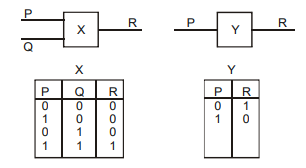
When the output of X is connected to the input of Y, the resulting combination is equivalent to a single:
1. NOT gate
2. OR gate
3. NAND gate
4. AND gate
© 2024 GoodEd Technologies Pvt. Ltd.