
 Q. No.
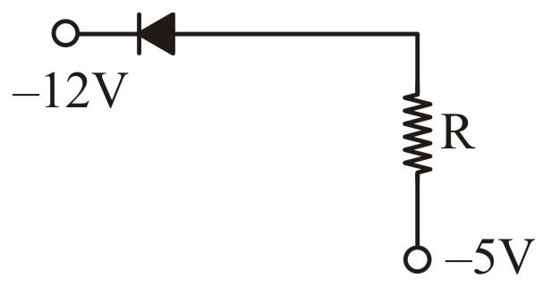
Of the diodes shown in the following diagrams, which one of the diodes is reverse biased?
1.

2.
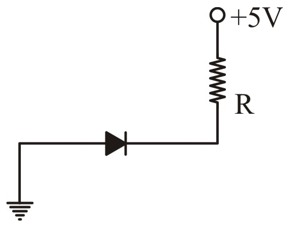
3.
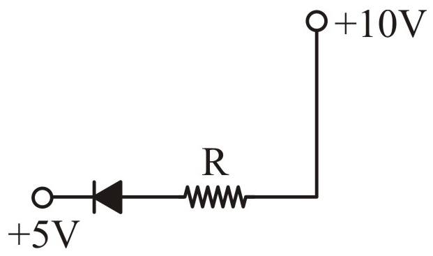
4.


The truth table for the following network is:

| 1. |
|
|||||||||||||||
| 2. |
|
|||||||||||||||
| 3. |
|
|||||||||||||||
| 4. | None of the above |
Zener diode is used as:
1. Half-wave rectifier
2. Full-wave rectifier
3. AC voltage stabilizer
4. DC voltage stabilizer


The depletion layer has (for an unbiased \(\mathrm{p\text-n}\) junction):
1. electrons
2. holes
3. static ions
4. neutral atoms
In semiconductors at room temperature:
| 1. | The valence band is completely filled and the conduction band is partially filled. |
| 2. | The valence band is completely filled. |
| 3. | The conduction band is completely empty. |
| 4. | The valence band is partially empty and the conduction band is partially filled. |
The peak voltage in the output of a half-wave diode rectifier fed with a sinusoidal signal without a filter is \(10\) V. The DC component of the output voltage is:
1. \(\frac{10}{\pi }\) V
2. \(10\) V
3. \(\frac{20}{\pi }\) V
4. \(\frac{10}{\sqrt{2}}\) V
In a p–n junction photocell, the value of the photo electromotive force produced by monochromatic light is proportional to:
| 1. | the intensity of the light falling on the cell. |
| 2. | the frequency of the light falling on the cell. |
| 3. | the voltage applied at the p–n junction. |
| 4. | the barrier voltage at the p–n junction. |
The output of the OR gate is \(1\):
| 1. | if either or both inputs are \(1.\) |
| 2. | only if both inputs are \(1.\) |
| 3. | if either input is zero |
| 4. | if both inputs are zero |
| 1. | High potential at the \(\mathrm{n}\) side and low potential at the \(\mathrm{p}\) side. |
| 2. | High potential at the \(\mathrm{p}\) side and low potential at the \(\mathrm{n}\) side. |
| 3. | \(\mathrm{p}\) and \(\mathrm{n}\) both are at the same potential. |
| 4. | Undetermined. |
| A | B | Y |
| \(1\) | \(1\) | \(0\) |
| \(0\) | \(1\) | \(1\) |
| \(1\) | \(0\) | \(1\) |
| \(0\) | \(0\) | \(1\) |
2. XOR
3. NOR
4. OR
© 2024 GoodEd Technologies Pvt. Ltd.