Select Chapter Topics:

 Q. No.
Which logic gate is represented by the following combination of logic gates?

1. OR
2. NAND
3. AND
4. NOR
1. OR
2. NAND
3. AND
4. NOR


Subtopic: Logic gates |
69%
From NCERT
NEET - 2015
To view explanation, please take trial in the course.
NEET 2025 - Target Batch
Hints
To view explanation, please take trial in the course.
NEET 2025 - Target Batch

In a \(\mathrm{p\text-n}\) junction diode not connected to any circuit:
| 1. | the potential is the same everywhere. |
| 2. | the \(\mathrm{p}\text-\)type is at higher potential than the \(\mathrm{n}\text-\)type side. |
| 3. | there is an electric field at the junction directed from the \(\mathrm{n}\text-\)type side to the \(\mathrm{p}\text-\)type side. |
| 4. | there is an electric field at the junction directed from the \(\mathrm{p}\text-\)type side to the \(\mathrm{n}\text-\)type side. |
Subtopic: PN junction |
59%
From NCERT
To view explanation, please take trial in the course.
NEET 2025 - Target Batch
Hints
To view explanation, please take trial in the course.
NEET 2025 - Target Batch
When a forward bias is applied to a \(\mathrm{p\text-n}\) junction, then what happens to the potential barrier \(V_B,\) and the width of charge depleted region \(x\)?
| 1. | \(V_B\) increases, \(x\) decreases | 2. | \(V_B\) decreases, \(x\) increases |
| 3. | \(V_B\) increases, \(x\) increases | 4. | \(V_B\) decreases, \(x\) decreases |
Subtopic: PN junction |
69%
From NCERT
To view explanation, please take trial in the course.
NEET 2025 - Target Batch
Hints
To view explanation, please take trial in the course.
NEET 2025 - Target Batch


Which of the energy band diagrams shown in the figure corresponds to that of a semiconductor?
| 1. |  |
2. |  |
| 3. |  |
4. |  |
Subtopic: Energy Band theory |
55%
From NCERT
To view explanation, please take trial in the course.
NEET 2025 - Target Batch
Hints
To view explanation, please take trial in the course.
NEET 2025 - Target Batch
The current through an ideal \(\mathrm{p\text-n}\) junction diode shown in the circuit will be:

| 1. | \(5\) A | 2. | \(0.2\) A |
| 3. | \(0.6\) A | 4. | zero |
Subtopic: PN junction |
65%
From NCERT
To view explanation, please take trial in the course.
NEET 2025 - Target Batch
Hints
To view explanation, please take trial in the course.
NEET 2025 - Target Batch
A potential barrier of \(0.50\) V exists across a \(\mathrm{p\text-n}\) junction. If the depletion region is \(5.0\times10^{-7}~\text{m}\) wide, the intensity of the electric field in this region is:
| 1. | \(1.0 \times 10^6 ~\text{V/m}\) | 2. | \(1.0 \times 10^5 ~\text{V/m}\) |
| 3. | \(2.0 \times 10^5 ~\text{V/m}\) | 4. | \(2.0 \times 10^6 ~\text{V/m}\) |
Subtopic: PN junction |
82%
From NCERT
To view explanation, please take trial in the course.
NEET 2025 - Target Batch
Hints
To view explanation, please take trial in the course.
NEET 2025 - Target Batch


Subtopic: Logic gates |
75%
From NCERT
To view explanation, please take trial in the course.
NEET 2025 - Target Batch
Hints
To view explanation, please take trial in the course.
NEET 2025 - Target Batch
A Zener diode is shown in the following circuit diagram. When the source voltage fluctuates such that \(V>V_z\) then:
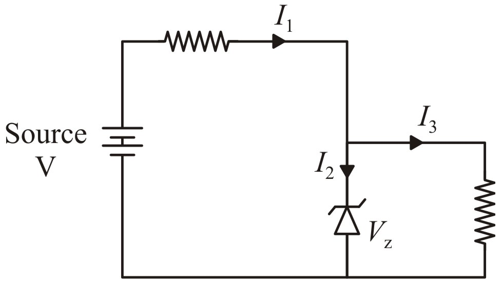
| 1. | all the current \(I_1, I_2~\text{and}~I_3\) change. |
| 2. | only \(I_1\) and \(I_2\) change and \(I_3\) remains constant. |
| 3. | only \(I_1\) and \(I_3\) change and \(I_2\) remains constant. |
| 4. | all the currents remain constant. |
Subtopic: Applications of PN junction |
69%
From NCERT
To view explanation, please take trial in the course.
NEET 2025 - Target Batch
Hints
To view explanation, please take trial in the course.
NEET 2025 - Target Batch
The net charges on -type semiconductor and -type semiconductor are, respectively:
| 1. | Positive, negative | 2. | Negative, positive |
| 3. | Positive, positive | 4. | Zero, zero |
Subtopic: Types of Semiconductors |
67%
From NCERT
To view explanation, please take trial in the course.
NEET 2025 - Target Batch
Hints
To view explanation, please take trial in the course.
NEET 2025 - Target Batch
In which of the following condition, diffusion current in \(\mathrm{p\text-n}\) junction is more than drift current?
| 1. | Forward biasing | 2. | Reverse biasing |
| 3. | No biasing | 4. | All of these |
Subtopic: PN junction |
73%
From NCERT
To view explanation, please take trial in the course.
NEET 2025 - Target Batch
Hints
To view explanation, please take trial in the course.
NEET 2025 - Target Batch
Select Chapter Topics:
© 2024 GoodEd Technologies Pvt. Ltd.