 Q. No.
In forward biasing of the p-n junction:
1. the positive terminal of the battery is connected to p-side and the depletion region becomes thick
2. the negative terminal of the battery is connected to n-side and the depletion region becomes thin
3. the positive terminal of the battery is connected to n-side and the depletion region become thin
4. the negative terminal of the battery is connected to p-side and the depletion region becomes thick


To unlock all the explanations of 6 chapters you need to be enrolled in MasterClass Course.
To unlock all the explanations of 6 chapters you need to be enrolled in MasterClass Course.

A transistor is operated in common emitter configuration at Vc =2V such that a change in the base current from 100 to 300 produces a change in the collector current from 10 mA to 20mA. The current gain is:
1. 75
2. 100
3. 25
4. 50
To unlock all the explanations of 6 chapters you need to be enrolled in MasterClass Course.
To unlock all the explanations of 6 chapters you need to be enrolled in MasterClass Course.
Which one of the following statements is false?
1. Pure Si doped with trivalent impurities gives a p-type semiconductor.
2. The majority carriers in an n-type semiconductor are holes.
3. The minority carriers in a p-type semiconductor are electrons.
4. The resistance of intrinsic semiconductor decreases with an increase in temperature.of
To unlock all the explanations of 6 chapters you need to be enrolled in MasterClass Course.
To unlock all the explanations of 6 chapters you need to be enrolled in MasterClass Course.


The device that can act as a complete electronic circuit is:
1. Junction diode
2. Integrated circuit
3. Junction transistor
4. Zener diode
To unlock all the explanations of 6 chapters you need to be enrolled in MasterClass Course.
To unlock all the explanations of 6 chapters you need to be enrolled in MasterClass Course.
A common emitter amplifier has a voltage gain of 50, an input impedance of 100 Ω and an output impedance of 200 Ω. The power gain of the amplifier is:
1. 500
2. 1000
3. 1250
4. 50
To unlock all the explanations of 6 chapters you need to be enrolled in MasterClass Course.
To unlock all the explanations of 6 chapters you need to be enrolled in MasterClass Course.
2. 4000 nm
3. 6000 nm
4. 4000 Å
To unlock all the explanations of 6 chapters you need to be enrolled in MasterClass Course.
To unlock all the explanations of 6 chapters you need to be enrolled in MasterClass Course.


A p-n photodiode is made of a material with a bandgap of 2.0 eV. The minimum frequency of the radiation that can be absorbed by the material is nearly:
1.
2.
3.
4.
To unlock all the explanations of 6 chapters you need to be enrolled in MasterClass Course.
To unlock all the explanations of 6 chapters you need to be enrolled in MasterClass Course.
To unlock all the explanations of 6 chapters you need to be enrolled in MasterClass Course.
To unlock all the explanations of 6 chapters you need to be enrolled in MasterClass Course.
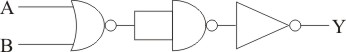
In the following circuit, the output Y for all possible inputs A and B is expressed by the truth table:

1. A B Y
0 0 0
0 1 0
1 0 0
1 1 1
2. A B Y
0 0 1
0 1 1
1 0 1
1 1 0
3. A B Y
0 0 1
0 1 0
1 0 0
1 1 1
4. A B Y
0 0 0
0 1 1
1 0 1
1 1 1
To unlock all the explanations of 6 chapters you need to be enrolled in MasterClass Course.
To unlock all the explanations of 6 chapters you need to be enrolled in MasterClass Course.


In the energy band diagram of a material shown below, the open circles and filled circles denote holes and electrons respectively. The material is a/an:

| 1. | \(\mathrm{p}\text-\)type semiconductor |
| 2. | insulator |
| 3. | metal |
| 4. | \(\mathrm{n}\text-\)type semiconductor |
To unlock all the explanations of 6 chapters you need to be enrolled in MasterClass Course.
To unlock all the explanations of 6 chapters you need to be enrolled in MasterClass Course.
© 2025 GoodEd Technologies Pvt. Ltd.