The following figure shows a logic gate circuit with two inputs A and B and the output C. The voltage waveforms of A, B, and C as shown below:
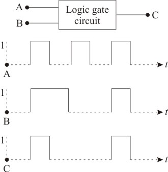
The logic circuit gate is :
1. AND gate
2. NAND gate
3. NOR gate
4. OR gate

The logic circuit gate is :

To unlock all the explanations of 14 chapters you need to be enrolled in MasterClass Course.

To unlock all the explanations of 14 chapters you need to be enrolled in MasterClass Course.
For a p-type semiconductor, which of the following statements is true?
1. Electrons are the majority carriers and pentavalent atoms are the dopants.
2. Electrons are the majority carriers and trivalent atoms are the dopants.
3. Holes are the majority carriers and trivalent atoms are the dopants.
4. Holes are the majority carriers and pentavalent atoms are the dopants.

To unlock all the explanations of 14 chapters you need to be enrolled in MasterClass Course.

To unlock all the explanations of 14 chapters you need to be enrolled in MasterClass Course.
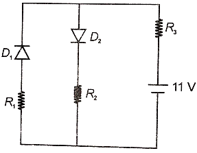
The ideal diodes are connected in the two branches as shown in the figure.. Current through the battery is:
1. 2A
2. 1A
3. 3A
4. 4A

To unlock all the explanations of 14 chapters you need to be enrolled in MasterClass Course.

To unlock all the explanations of 14 chapters you need to be enrolled in MasterClass Course.
Zener diodes with breakdown voltage ranging over 2 V — 200 V are commercially available. The breakdown voltage of a Zener diode:
1. Increases with increasing doping concentration
2. Decreases with increasing doping concentration
3. Does not depend on doping concentration
4. May increase or decrease with increasing doping concentration

To unlock all the explanations of 14 chapters you need to be enrolled in MasterClass Course.

To unlock all the explanations of 14 chapters you need to be enrolled in MasterClass Course.
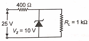
A Zener diode of breakdown voltage, = 10 V is used in the given circuit. The current through the load resistor is:
1. 10
2. 5
3. 10 mA
4. 5 mA

To unlock all the explanations of 14 chapters you need to be enrolled in MasterClass Course.

To unlock all the explanations of 14 chapters you need to be enrolled in MasterClass Course.
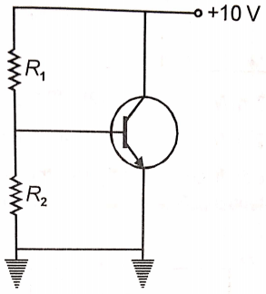
The figure shows an n-p-n transistor. Choose the correct statement out of the following.
1. Collector-base junction, as well as emitter-base junction both, are forward biased.
2. Collector-base junction, as well as emitter-base junction both, are reverse biased.
3. Collector-base junction is forward biased and the emitter-base junction is reverse biased.
4. Collector-base junction is reverse-biased and the emitter-base junction is forward biased.

To unlock all the explanations of 14 chapters you need to be enrolled in MasterClass Course.

To unlock all the explanations of 14 chapters you need to be enrolled in MasterClass Course.
In the circuit shown in the figure, the current amplification factor () is 80. Neglecting base-
emitter voltage (), calculate the collector current :
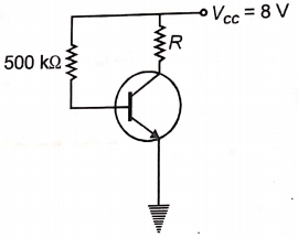
1. 0.78 mA
2. 0.96 mA
3. 1.28 mA
4. 2.20 mA

To unlock all the explanations of 14 chapters you need to be enrolled in MasterClass Course.

To unlock all the explanations of 14 chapters you need to be enrolled in MasterClass Course.
In the circuit shown, if each diode has a forward-biased resistance of 75 and infinite resistance in reverse biasing, what will be the values of currents ?
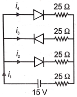
1.
2.
3.
4.

To unlock all the explanations of 14 chapters you need to be enrolled in MasterClass Course.

To unlock all the explanations of 14 chapters you need to be enrolled in MasterClass Course.
Doping of a semiconductor (with small traces of impurity atoms) generally changes the resistivity as follows:
1. does not alter
2. increases
3. decreases
4. may increase or decrease depending on the dopant

To unlock all the explanations of 14 chapters you need to be enrolled in MasterClass Course.

To unlock all the explanations of 14 chapters you need to be enrolled in MasterClass Course.
Given below are four logic gate symbols (figure). Those for OR, NOR, and NAND are respectively-
1. 
2. 
3. 
4. 
1. 1, 4, 3
2. 4, 1, 2
3. 1, 3, 4
4. 4, 2, 1

To unlock all the explanations of 14 chapters you need to be enrolled in MasterClass Course.

To unlock all the explanations of 14 chapters you need to be enrolled in MasterClass Course.


