When a forward bias is applied to a P–N junction, then what happens to the potential barrier VB, and the width of depletion region x?
1. VB increases, x decreases
2. VB decreases, x increases
3. VB increases, x increases
4. VB decreases, x decreases

To unlock all the explanations of 14 chapters you need to be enrolled in MasterClass Course.

To unlock all the explanations of 14 chapters you need to be enrolled in MasterClass Course.

To unlock all the explanations of 14 chapters you need to be enrolled in MasterClass Course.

To unlock all the explanations of 14 chapters you need to be enrolled in MasterClass Course.
For the transistor circuit shown below, if = 100, voltage drop between emitter and base is 0.7V then value of VCE will be :
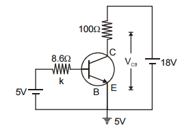
1. 10 V
2. 5 V
3. 13 V
4. 0

To unlock all the explanations of 14 chapters you need to be enrolled in MasterClass Course.

To unlock all the explanations of 14 chapters you need to be enrolled in MasterClass Course.

To unlock all the explanations of 14 chapters you need to be enrolled in MasterClass Course.

To unlock all the explanations of 14 chapters you need to be enrolled in MasterClass Course.
Ge and Si diodes conduct at 0.3 V and 0.7 V respectively. In the following figure if Ge diode connection is reversed, the value of V0 changes by:
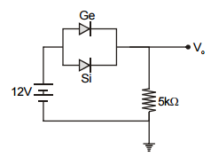
1. 0.2 V
2. 0.4 V
3. 0.6 V
4. 0.8 V

To unlock all the explanations of 14 chapters you need to be enrolled in MasterClass Course.

To unlock all the explanations of 14 chapters you need to be enrolled in MasterClass Course.
Given circuit work as a full wave rectifier then input and output terminals will be respectively:-
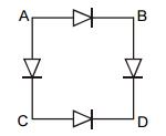
1. A, D and B, C
2. B, C and A, D
3. A, B and C, D
4. A, C and B, C

To unlock all the explanations of 14 chapters you need to be enrolled in MasterClass Course.

To unlock all the explanations of 14 chapters you need to be enrolled in MasterClass Course.
In the circuit shown in the figure, when the input voltage of base resistance is 10V, VBE is zero and VCE is also zero then what is the value of ?
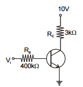
1. 133
2. 1330
3. 13.3
4. 1.33

To unlock all the explanations of 14 chapters you need to be enrolled in MasterClass Course.

To unlock all the explanations of 14 chapters you need to be enrolled in MasterClass Course.
The logic circuit shown has the input waveforms 'A' and 'B' as shown. Pick out the CORRECT output waveform :-
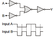
1. 
2. 
3. 
4. 

To unlock all the explanations of 14 chapters you need to be enrolled in MasterClass Course.

To unlock all the explanations of 14 chapters you need to be enrolled in MasterClass Course.
The circuit shown here is logically equivalent to:

1. OR gate
2. AND gate
3. NOT gate
4. NAND gate

To unlock all the explanations of 14 chapters you need to be enrolled in MasterClass Course.

To unlock all the explanations of 14 chapters you need to be enrolled in MasterClass Course.
In an NPN transistor circuit, the collector current is 10 mA. If 90% of the electrons emitted reach the collector, the emitter current() and base current ( are given by):-
1.
2.
3.
4.

To unlock all the explanations of 14 chapters you need to be enrolled in MasterClass Course.

To unlock all the explanations of 14 chapters you need to be enrolled in MasterClass Course.


