
 Q. No.
In the following figure, the diodes which are forward biased, are
(I)

(II)
(III)

(IV)

Choose the correct option from the given ones:
1. III and IV only
2. I and III only
3. II only
4. II and IV only
(II)


| 1. | \(\mathrm{n}\text-\)type with electron concentration \(n_{e}=5\times10^{22}~\text{m}^{-3}\) |
| 2. | \(\mathrm{p}\text-\)type with electron concentration \(n_{e}=2.5\times10^{23}~\text{m}^{-3}\) |
| 3. | \(\mathrm{n}\text-\)type with electron concentration \(n_{e}=2.5\times10^{10}~\text{m}^{-3}\) |
| 4. | \(\mathrm{p}\text-\)type with electron concentration \(n_{e}=5\times10^{9}~\text{m}^{-3}\) |
A Zener diode, having breakdown voltage equal to \(15\) V, is used in a voltage regulator circuit, as shown in the figure. The current through the diode is:
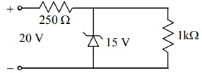
1. \(10\) mA
2. \(15\) mA
3. \(20\) mA
4. \(5\) mA


Which one of the following statement is false?
(1) Pure Si doped with trivalent impurities gives a p-type semiconductor
(2) Majority carries in a n-type semiconductor are holes
(3) Minority carries in a p-type semiconductor are electrons
(4) The resistance of intrinsic semiconductor decreases with increase of temperature

The device that can act as a complete electronic circuit is
1. Junction diode
2. Integrated circuit
3. Junction transistor
4. Zener diode
The following figure shows a logic gate circuit with two inputs A and B and the output Y. The voltage waveforms of A, B and Y are as given

The logic gate is
1. gate
2. gate
3. gate
4. gate


For transistor action:
| (a) | the base, emitter and collector regions should have similar size and doping concentrations. |
| (b) | the base regions must be very thin and lightly doped. |
| (c) | the emitter-base junction is forward biased and the base-collector junction is reverse biased. |
| (d) | both the emitter-base junction as well as the base-collector junction are forward biased. |
Which of the following pairs of statements is correct?
1. (d) and (a)
2. (a) and (b)
3. (b) and (c)
4. (c) and (d)
A p-n photodiode is fabricated from a semiconductor with a band gap of It can detect a signal of wavelength
1.
2.
3.
4.
The symbolic representation of four logic gates


(i) (ii)


(iii) (iv)
The logic symbols for and gates are respectively
1. (iii), (iv), (ii)
2. (iv), (i), (iii)
3. (iv), (ii), (i)
4. (i), (iii), (iv)


A transistor is operated in common-emitter configuration at such that a change in the base current from 100 to 200 produces a change in the collector current from 5 mA to 10 mA. The current gain is
1. 75
2. 100
3. 150
4. 50
© 2026 GoodEd Technologies Pvt. Ltd.