In case of a semiconductor, which of the following statement is wrong
(1) Doping increases conductivity
(2) Temperature coefficient of resistance is negative
(3) Resisitivity is in between that of a conductor and insulator
(4) At absolute zero temperature, it behaves like a conductor
In a P-type semiconductor, germanium is doped with
(1) Boron
(2) Gallium
(3) Aluminium
(4) All of these
Which is the correct relation for the forbidden energy gap in the conductor, semiconductor, and insulator
(1)
(2)
(3)
(4)
Which of the following has negative temperature coefficient of resistance
(1) Copper
(2) Aluminium
(3) Iron
(4) Germanium
The energy gap of silicon is 1.14 eV. The maximum wavelength at which silicon will begin absorbing energy is
(1) 10888 Å
(2) 1088.8 Å
(3) 108.88 Å
(4) 10.888 Å
Which of the energy band diagrams shown in the figure corresponds to that of a semiconductor?
| 1. |  |
2. |  |
| 3. |  |
4. |  |
The energy band diagrams for three semiconductor samples of silicon are as shown. We can then assert that-
1. Sample X is undoped while samples Y and Z have been doped with a third group and a fifth group impurity respectively
2. Sample X is undoped while both samples Y and Z have been doped with a fifth group impurity
3. Sample X has been doped with equal amounts of third and fifth group impurities while samples Y and Z are undoped
4. Sample X is undoped while samples Y and Z have been doped with a fifth group and a third group impurity respectively
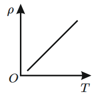
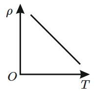
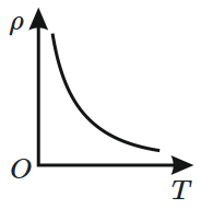
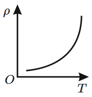
Which graph correctly represents how the resistivity \((\rho)\) of a semiconductor changes with temperature \((T)\text{?}\)
| 1. |  |
2. |  |
| 3. |  |
4. |  |
In the half-wave rectifier circuit shown. Which one of the following wave forms is true for , the output across C and D?
A full-wave rectifier circuit along with the input and output voltages is shown in the figure.
The contribution to the output voltage from diode – 2 is :
(1) A, C
(2) B, D
(3) B, C
(4) A, D


