A transistor is operated in common emitter configuration at such that a change in the base current from to produces a change in the collector current from to . The current gain is
1. 75 2. 100
3. 25 4. 50
In the following figure, the diodes which are forward biased, are


1. III and IV only
2. I and III only
3. II only
4. II and IV only
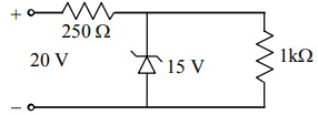
A Zener diode, having breakdown voltage equal to \(15\) V, is used in a voltage regulator circuit, as shown in the figure. The current through the diode is:

1. \(10\) mA
2. \(15\) mA
3. \(20\) mA
4. \(5\) mA
Which one of the following statement is false?
(1) Pure Si doped with trivalent impurities gives a p-type semiconductor
(2) Majority carries in a n-type semiconductor are holes
(3) Minority carries in a p-type semiconductor are electrons
(4) The resistance of intrinsic semiconductor decreases with increase of temperature
To get an output Y =1 from the circuit shown below, the input must be
A B C
1. 0 1 0
2. 0 0 1
3. 1 0 1
4. 1 0 0
The following figure shows a logic gate circuit with two inputs A and B and the output Y. The voltage waveforms of A, B and Y are as given

The logic gate is
1. gate
2. gate
3. gate
4. gate
For transistor action:
| (a) | the base, emitter and collector regions should have similar size and doping concentrations. |
| (b) | the base regions must be very thin and lightly doped. |
| (c) | the emitter-base junction is forward biased and the base-collector junction is reverse biased. |
| (d) | both the emitter-base junction as well as the base-collector junction are forward biased. |
Which of the following pairs of statements is correct?
1. (d) and (a)
2. (a) and (b)
3. (b) and (c)
4. (c) and (d)
A p-n photodiode is fabricated from a semiconductor with a band gap of It can detect a signal of wavelength
1.
2.
3.
4.
The circuit is equivalent to
1. AND gate 2. NAND gate
3. NOR gate 4. OR gate
In the forward bias arrangement of a PN-junction diode
(1) The N-end is connected to the positive terminal of the battery
(2) The P-end is connected to the positive terminal of the battery
(3) The direction of current is from N-end to P-end in the diode
(4) The P-end is connected to the negative terminal of battery


