
Transfer characteristics [output voltage () vs input voltage ()] for a base biased transistor in CE configurations are as shown in the figure. For using the transistor as a switch, it is used:

1. In region III
2. Both in the region (I) and (III)
3. In region II
4. In region I


The symbolic representation of four gates is shown as:
Pick out which ones are for AND, NAND, and NOT gates, respectively.

1. (i), (iv), and (iii)
2. (ii), (iii), and (iv)
3. (ii), (iv), and (iii)
4. (ii), (iv), and (i)
A transistor is operated in a common emitter configuration at Vc =2 V such that a change in the base current from 100 to 300 produces a change in the collector current from 10 mA to 20mA. The current gain is:
1. 75
2. 100
3. 25
4. 50


A common emitter amplifier has a voltage gain of 50, an input impedance of 100 Ω and an output impedance of 200 Ω. The power gain of the amplifier is:
1. 500
2. 1000
3. 1250
4. 50
To get an output Y = 1 from the circuit shown below, the input must be:

1. A=0 B=1 C=0
2. A=0 B=0 C=1
3. A=1 B=0 C=1
4. A=1 B=0 C=0
1. \(6000~\mathring{A}\)
2. \(4000~\text{nm}\)
3. \(6000~\text{nm}\)
4. \(4000~\mathring{A}\)


In the following circuit, the output \(Y\) for all possible inputs \(A\) and \(B\) is expressed by the truth table:

| 1. | A | B | Y | 2. | A | B | Y |
| 0 | 0 | 0 | 0 | 0 | 1 | ||
| 0 | 1 | 0 | 0 | 1 | 1 | ||
| 1 | 0 | 0 | 1 | 0 | 1 | ||
| 1 | 1 | 1 | 1 | 1 | 0 | ||
| 3. | 0 | 0 | 1 | 4. | 0 | 0 | 0 |
| 0 | 1 | 0 | 0 | 1 | 1 | ||
| 1 | 0 | 0 | 1 | 0 | 1 | ||
| 1 | 1 | 1 | 1 | 1 | 1 |
In the energy band diagram of a material shown below, the open circles and filled circles denote holes and electrons respectively. The material is a/an:
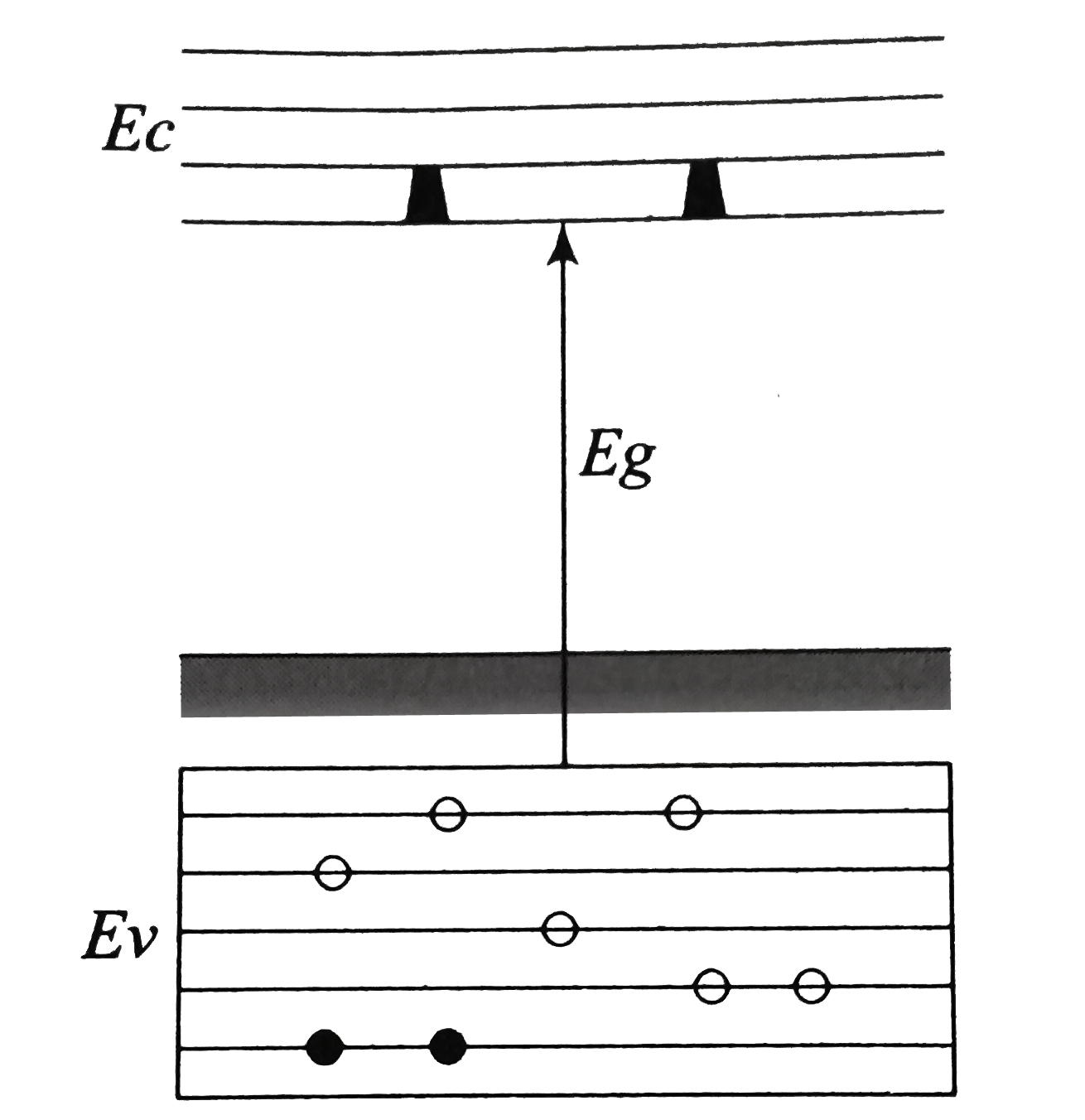
1. p-type semiconductor
2. insulator
3. metal
4. n-type semiconductor


A transistor is operated in a common emitter configuration at constant collector voltage Vc = 1.5 V such that a change in the base current from 100 μA to 150 μA produces a change in the collector current from 5 mA to 10 mA. The current gain (β) is:
1. 67
2. 75
3. 100
4. 50
© 2026 GoodEd Technologies Pvt. Ltd.