
 Q. No.
Choose the correct statement
(a) When we heat a semiconductor its resistance increases
(b) When we heat a semiconductor its resistance decreases
(c) When we cool a semiconductor to 0 K then it becomes super conductor
(d) Resistance of a semiconductor is independent of temperature
सही कथन का चयन कीजिए:
(a) जब हम किसी अर्धचालक को गर्म करते हैं, तो इसका प्रतिरोध बढ़ता है।
(b) जब हम किसी अर्धचालक को गर्म करते हैं, तो इसका प्रतिरोध घटता है।
(c) जब हम किसी अर्धचालक को 0 K तक ठंडा करते हैं, तो यह अतिचालक बन जाता है।
(d) अर्धचालक का प्रतिरोध तापमान से स्वतंत्र होता है।
(b) When we heat a semiconductor its resistance decreases
(c) When we cool a semiconductor to 0 K then it becomes super conductor
(d) Resistance of a semiconductor is independent of temperature
(b) जब हम किसी अर्धचालक को गर्म करते हैं, तो इसका प्रतिरोध घटता है।
(c) जब हम किसी अर्धचालक को 0 K तक ठंडा करते हैं, तो यह अतिचालक बन जाता है।
(d) अर्धचालक का प्रतिरोध तापमान से स्वतंत्र होता है।


Which of the energy band diagrams shown in the figure corresponds to that of a semiconductor
1. 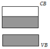
2. 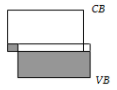
3. 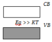
4. 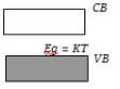
आरेख में दर्शाए गए ऊर्जा बैंड आरेखों में से कौन-सा अर्धचालक के संगत है?
1.
2.
3.
4.
In a semiconducting material, the mobilities of electrons and holes are and respectively. Which of the following is true?
(a) > (b) <
(c) = (d) <0; >0
अर्धचालकीय पदार्थ में, इलेक्ट्रॉनों और कोटरों की गतिशीलता क्रमशः और है। निम्नलिखित में से कौन-सा सत्य है?
(a) > (b) <
(c) = (d) <0; >0


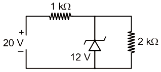
For the transistor circuit shown below, if = 100, voltage drop between emitter and base is 0.7 V, then value of will be :

1. 10 V
2. 5 V
3. 13 V
4. 0 V
निम्नवत दर्शाए गए ट्रांजिस्टर परिपथ के लिए, यदि = 100, उत्सर्जक और आधार के बीच विभव पतन 0.7 V है, तब का मान कितना होगा?
1. 10 V
2. 5 V
3. 13 V
4. 0 V
The current through an ideal p-n junction diode shown in the circuit will be -
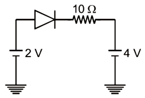
1. 5 A
2. 0.2 A
3. 0.6 A
4. Zero
परिपथ में दर्शाए गए आदर्श p-n संधि डायोड में धारा की गणना कीजिए।

1. 5 A
2. 0.2 A
3. 0.6 A
4. शून्य
In the given circuit power developed in \(1 k \Omega\) resistor is

1. 36 mW
2. 12 mW
3. 144 mW
4. 64 mW
दिए गए परिपथ में \(1 k \Omega\) प्रतिरोधक में उत्पन्न शक्ति है:
1. 36 mW
2. 12 mW
3. 144 mW
4. 64 mW


The diode shown in the circuit is a silicon diode. The potential difference between the points A and B will be
(a) 6 V

(b) 0.6 V
(c) 0.7 V
(d) 0 V
परिपथ में दर्शाया गया डायोड एक सिलिकॉन डायोड है। बिंदु A और B के मध्य विभवांतर कितना होगा?
(a) 6 V
(b) 0.6 V
(c) 0.7 V
(d) 0 V
In a common base amplifier the phase difference between the input signal voltage and the output voltage is
(a) 0 (b)
(c) (d)
उभयनिष्ठ आधार प्रवर्धक में निवेशी सिग्नल वोल्टेज और निर्गत वोल्टेज के मध्य कलांतर की गणना कीजिए:
(a) 0 (b)
(c) (d)
The transfer ratio of a transistor is 50. The input resistance of the transistor when used in the common-emitter configuration is 1 K. The peak value for an A.C input voltage of 0.01 V peak is
| 1. | 100 μ A | 2. | 0.01 mA |
| 3. | 0.25 mA | 4. | 500 μ A |
ट्रांजिस्टर का परिणमन अनुपात 50 है। उभयनिष्ठ उत्सर्जक विन्यास में उपयोग किए जाने पर ट्रांजिस्टर का निवेशी प्रतिरोध 1K है। 0.01 V के अधिकतम मान की प्रत्यावर्ती निवेशी वोल्टता के लिए प्रत्यावर्ती संग्राहक धारा का अधिकतम मान ज्ञात कीजिए।
| 1. | 100 μ A | 2. | 0.01 mA |
| 3. | 0.25 mA | 4. | 500 μ A |


In the following circuit, find and .

(a) 0, 0
(b) 5 mA, 5 mA
(c) 5 mA, 0
(d) 0, 5 mA
निम्नलिखित परिपथ में, और ज्ञात कीजिए:
(a) 0, 0
(b) 5 mA, 5 mA
(c) 5 mA, 0
(d) 0.5 mA
© 2026 GoodEd Technologies Pvt. Ltd.