
 Q. No.
In the diagram, the input is across the terminals A and C and the output is across the terminals B and D, then the output is

1.
Zero
2.
Same as input
3.
Full wave rectifier
4.
Half wave rectifier
आरेख में, निवेशी, शीर्षों A और C के मध्य है और निर्गत, शीर्षों B और D के मध्य है, तब निर्गत है -
1.
शून्य
2.
निवेशी के समान
3.
पूर्ण तरंग दिष्टकारी
4.
अर्ध तरंग दिष्टकारी


In an NPN transistor the collector current is 24 mA. If 80% of electrons reach collector its base current in mA is
| 1. | 36 | 2. | 26 |
| 3. | 16 | 4. | 6 |
NPN ट्रांजिस्टर में संग्राहक धारा 24 mA है। यदि 80% इलेक्ट्रॉन संग्राहक तक पहुंचते हैं, तब इसकी आधार धारा mA में ज्ञात कीजिए।
| 1. | 36 | 2. | 26 |
| 3. | 16 | 4. | 6 |
The voltage gain of an amplifier with 9% negative feedback is 10. The voltage gain without feedback will be
(a) 90 (b) 10
(c) 1.25 (d) 100
9% ऋणात्मक पुनर्भरण के साथ प्रवर्धक का वोल्टेज लाभ 10 है। पुनर्भरण के बिना वोल्टेज लाभ कितना होगा?
(a) 90 (b) 10
(c) 1.25 (d) 100


C and Si both have same lattice structure,having 4 bonding electrons in each.However, C is insulator whereas Si is intrinsic semiconductor. This is because
| 1. | in case of C, the valence band is not completely filled at absolute zero temperature |
| 2. | in case of C,the condition band is partly filled even at absolute zero temperature |
| 3. | the four bonding electrons in the case of C lie in the second orbit,Whereas in the case of Si they lie in the third |
| 4. | the four bonding electrons in the case of C lie in the third orbit, whereas for Si they lie in the fourth orbit |
C और Si दोनों में समान जालक संरचना है, जिसमें प्रत्येक में 4 बंधित इलेक्ट्रॉन हैं। हालांकि, C विद्युतरोधी है जबकि Si नैज अर्धचालक है। यह किस कारण है?
| 1. | C की स्थिति में संयोजकता बैंड परम शून्य ताप पर पूर्ण रूप से भरा नहीं होता है। |
| 2. | C की स्थिति में चालक बैंड परम शून्य ताप पर भी आंशिक रूप से भरा हुआ होता है। |
| 3. | C की स्थिति में चार बंधित इलेक्ट्रॉन दूसरी कक्षा में स्थित हैं, जबकि Si की स्थिति में वे तीसरी कक्षा में स्थित हैं। |
| 4. | C की स्थिति में चार बंधित इलेक्ट्रॉन तीसरी कक्षा में स्थित हैं, जबकि Si की स्थिति में वे चौथी कक्षा में स्थित हैं। |
The following configuration of the logic gate is equivalent to
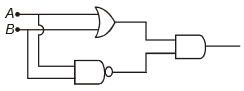
1. NAND gate
2. XOR gate
3. OR gate
4. NOR gate
लॉजिक गेट का निम्नलिखित विन्यास किसके समतुल्य है?

1. NAND गेट
2. XOR गेट
3. OR गेट
4. NOR गेट
In a common emitter transistor amplifier, the audio signal voltage across resistance of 1 k is 2V. If the base resistance is 200 and the current amplification factor is 50, the input signal voltage will be
(1) 4 mV
(2) 8 mV
(3) 16 mV
(4) 32 mV
एक उभयनिष्ठ उत्सर्जक ट्रांजिस्टर प्रवर्धक में, 1k के प्रतिरोध के सिरों पर श्रव्य सिग्नल वोल्टता 2V है। यदि आधार प्रतिरोध 200 है और धारा प्रवर्धन गुणांक 50 है, निवेशी सिग्नल वोल्टता होगी
(1) 4 mV
(2) 8 mV
(3) 16mV
(4) 32 mV


If a small amount of aluminium is added to the silicon crystal
1. Its resistance is decreased
2. It becomes a p-type semiconductor
3. There will be less free-electron than holes in semiconductor
4. All of these are correct
यदि ऐलुमिनियम की थोड़ी मात्रा को सिलिकॉन क्रिस्टल में मिलाया जाता है, तो -
1. इसका प्रतिरोध घटता है।
2. यह p-प्रकार का अर्धचालक बन जाता है।
3. अर्धचालक में कोटरों की तुलना में मुक्त-इलेक्ट्रॉन कम होंगे।
4. ये सभी सत्य हैं।
1.
2.
3.
4. All of these
यदि उभयनिष्ठ आधार विन्यास में ट्रांजिस्टर का धारा लाभ है और उभयनिष्ठ उत्सर्जक विन्यास में धारा लाभ है, तब -
1.
2.
3.
4. ये सभी
To get output 1 for the following circuit, the correct choice for the input is
(a) (b)
(c) (d)
निम्नलिखित परिपथ के लिए निर्गत 1 प्राप्त करने के लिए, निवेशी के लिए सही विकल्प कौन-सा है?
(a) (b)
(c) (d)


If in a p-n junction, a square input signal of 10V is applied as shown,
then the output across RL will be
(a) (b)

(d)

यदि p-n संधि में, 10V के वर्गाकर निवेशी संकेत को दर्शाए गए अनुसार आरोपित किया गया है,
तब RL में निर्गत वोल्टेज कितना होगा?
(a) (b)
(d)
© 2025 GoodEd Technologies Pvt. Ltd.