
 Q. No.
Which logic gate is represented by the following combination of logic gates

(1) OR
(2) NAND
(3) AND
(4) NOR
लॉजिक गेट के निम्नलिखित संयोजन द्वारा किस लॉजिक गेट को दर्शाया जाता है?
(1) OR
(2) NAND
(3) AND
(4) NOR


Symbolic representation of four logic gates
are shown as
(i)

(ii)

(iii)

(iv)

Pick out which ones are for AND, NAND and
NOT gates, respectively.
(a) (iii), (ii)and (i)
(b) (iii), (ii) and (iv)
(c) (ii), (iv) and (iii)
(d) (ii), (iii) and (iv)
चार लॉजिक गेटों के प्रतीकात्मक निरूपण को निम्न रूप में दर्शाया गया हैं:
(i)
(ii)
(iii)
(iv)
उनका चयन कीजिए, जो क्रमशः AND, NAND और NOT के लिए हैं:
(a) (iii), (ii) और (i)
(b) (iii), (ii) और (iv)
(c) (ii), (iv) और (iii)
(d) (ii), (iii) और (iv)
When a p-n junction is forward biased:
1. Depletion region becomes thick
2. p-side is at a higher potential than n side
3. Current flowing is zero
4. Effective resistance is of the order of
जब p-n संधि अग्र अभिनत होता है:
1. अवक्षय क्षेत्र मोटा हो जाता है।
2. p-क्षेत्र, n क्षेत्र की तुलना में उच्च विभव पर है।
3. धारा प्रवाह शून्य है।
4. प्रभावी प्रतिरोध कोटि का है।


When a transistor is used as a switch it is in:
1. Active state
2. Cut off state
3. Saturation state
4. Both cut off state and saturation state are possible
जब ट्रांजिस्टर का उपयोग स्विच के रूप में किया जाता है, तब यह किस अवस्था में होता है?
1. सक्रिय अवस्था
2. भंजन अवस्था
3. संतृप्ति अवस्था
4. भंजन अवस्था और संतृप्ति अवस्था दोनों संभव हैं।
In semiconductors, which of the following gives the law of mass action (where symbols have their usual meanings)-
1.
2.
3.
4.
अर्धचालकों में, निम्नलिखित में से कौन-सा द्रव्यमान प्रतिक्रिया के नियम (जहां चिन्हों के अपने सामान्य अर्थ हैं) को दर्शाता है?
1.
2.
3.
4.
If , , are the lengths of the emitter, base and collector of a transistor then
(a)= = (b) <>
(c) < < (d) > >
यदि , , उत्सर्जक, आधार और संग्राहक की लंबाई है, तब -
(a)= = (b) <>
(c) < < (d) > >


GaAs is
(a) Element semiconductor
(b) Alloy semiconductor
(c) Bad conductor
(d) Metallic semiconductor
GaAs क्या है?
(a) तत्व अर्धचालक
(b) मिश्रधातु अर्धचालक
(c) कुचालक
(d) धात्विक अर्धचालक
The phase difference between input and output voltages of a CE circuit is
(a) 0 (b) 90
(c) 180 (d) 270
CE परिपथ के निवेश और निर्गत वोल्टेज के मध्य कलांतर की गणना कीजिए:
(a) 0 (b) 90
(c) 180 (d) 270
Choose the correct statement
(a) When we heat a semiconductor its resistance increases
(b) When we heat a semiconductor its resistance decreases
(c) When we cool a semiconductor to 0 K then it becomes super conductor
(d) Resistance of a semiconductor is independent of temperature
सही कथन का चयन कीजिए:
(a) जब हम किसी अर्धचालक को गर्म करते हैं, तो इसका प्रतिरोध बढ़ता है।
(b) जब हम किसी अर्धचालक को गर्म करते हैं, तो इसका प्रतिरोध घटता है।
(c) जब हम किसी अर्धचालक को 0 K तक ठंडा करते हैं, तो यह अतिचालक बन जाता है।
(d) अर्धचालक का प्रतिरोध तापमान से स्वतंत्र होता है।


Which of the energy band diagrams shown in the figure corresponds to that of a semiconductor
1. 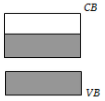
2. 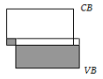
3. 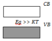
4. 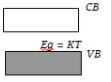
आरेख में दर्शाए गए ऊर्जा बैंड आरेखों में से कौन-सा अर्धचालक के संगत है?
1.
2.
3.
4.
© 2026 GoodEd Technologies Pvt. Ltd.