
 Q. No.
Pure Si at 500 K has equal number of electron and hole concentrations of Doping by indium increases to The doped semiconductor is of
1. n-type with electron concentration
2. p-type with electron concentration
3. n-type with electron concentration
4. p-type with electron concentration
500 K पर शुद्ध Si में इलेक्ट्रॉन और कोटरों की संख्या के बराबर है। इंडियम द्वारा अपमिश्रण कोटरों की संख्या को तक बढ़ा देता है। अपमिश्रित अर्धचालक किस प्रकार का अर्धचालक है?
1. इलेक्ट्रॉन सांद्रता के साथ n-प्रकार का अर्धचालक
2. इलेक्ट्रॉन सांद्रता के साथ p-प्रकार का अर्धचालक
3. इलेक्ट्रॉन सांद्रता के साथ n-प्रकार का अर्धचालक
4. इलेक्ट्रॉन सांद्रता के साथ p-प्रकार का अर्धचालक


A Zener diode, having breakdown voltage equal to 15 V, is used in a voltage regulator circuit shown in the figure. The current through the diode is :

| 1. | 10 mA | 2. | 15 mA |
| 3. | 20 mA | 4. | 5 mA |
एक ज़ेनर डायोड, जिसकी भंजक वोल्टता 15V के बराबर है, का उपयोग आरेख में दर्शाए गए वोल्टता नियंत्रक परिपथ में किया जाता है। डायोड के माध्यम में धारा ज्ञात कीजिए:
| 1. | 10 mA | 2. | 15 mA |
| 3. | 20 mA | 4. | 5 mA |
For transistor action
| 1 | Base, emitter and collector regions should have similar size and doping concentrations. |
| 2 | The base regions must be very thin and lightly doped. |
| 3 | The emitter-base junction is forward biased and the base-collector junction is reverse biased. |
| 4 | Both the emitter-base junction as well as the base-collector junction are forward biased. |
Which of the following pairs of statements is correct?
1. (4) and (1)
2. (1) and (2)
3. (2) and (3)
4. (3) and (4)
ट्रांजिस्टर की क्रिया के लिए -
| 1 | आधार, उत्सर्जक और संग्राहक क्षेत्रों का आकार और अपमिश्रण सांद्रता समान होनी चाहिए। |
| 2 | आधार क्षेत्र बहुत पतला और कम अपमिश्रित होना चाहिए। |
| 3 | उत्सर्जक-आधार संधि अग्र अभिनत है और आधार-संग्राहक संधि पश्च अभिनत है। |
| 4 | उत्सर्जक-आधार संधि और आधार-संग्राहक संधि दोनों ही अग्र अभिनत हैं। |
निम्नलिखित में से कौन सा कथन युग्म सही है?
1. (4) और (1)
2. (1) और (2)
3. (2) और (3)
4. (3) और (4)


Two PN-junctions can be connected in series by three different methods as shown in the figure. If the potential difference in the junctions is the same, then the correct connections will be

1. In the circuit (1) and (2)
2. In the circuit (2) and (3)
3. In the circuit (1) and (3)
4. Only in the circuit (1)
दो PN-संधियों को आरेख में दर्शाए गए अनुसार तीन अलग-अलग विधियों से जोड़ा जा सकता है। यदि संधियों में विभवांतर समान है, तब सही संयोजन होगा-
1. परिपथ (1) और (2) में
2. परिपथ (2) और (3) में
3. परिपथ (1) और (3) में
4. केवल परिपथ (1) में
The approximate ratio of resistances in the forward and reverse bias of the PN-junction diode is:
(a) (b)
(c) (d)
अग्र अभिनत और पश्च अभिनत में PN-संधि डायोड के प्रतिरोधों का सन्निकट अनुपात ज्ञात कीजिए।
(a) (b)
(c) (d)
In the diagram, the input is across the terminals A and C and the output is across the terminals B and D, then the output is

| 1. | Zero | 2. | Same as input |
| 3. | Full wave rectifier | 4. | Half wave rectifier |
आरेख में, निवेशी, शीर्षों A और C के मध्य है और निर्गत, शीर्षों B और D के मध्य है, तब निर्गत है -
| 1. | शून्य |
| 2. | निवेशी के समान |
| 3. | पूर्ण तरंग दिष्टकारी |
| 4. | अर्ध तरंग दिष्टकारी |


In an NPN transistor the collector current is 24 mA. If 80% of electrons reach collector its base current in mA is
| 1. | 36 | 2. | 26 |
| 3. | 16 | 4. | 6 |
NPN ट्रांजिस्टर में संग्राहक धारा 24 mA है। यदि 80% इलेक्ट्रॉन संग्राहक तक पहुंचते हैं, तब इसकी आधार धारा mA में ज्ञात कीजिए।
| 1. | 36 | 2. | 26 |
| 3. | 16 | 4. | 6 |
The voltage gain of an amplifier with 9% negative feedback is 10. The voltage gain without feedback will be
(a) 90 (b) 10
(c) 1.25 (d) 100
9% ऋणात्मक पुनर्भरण के साथ प्रवर्धक का वोल्टेज लाभ 10 है। पुनर्भरण के बिना वोल्टेज लाभ कितना होगा?
(a) 90 (b) 10
(c) 1.25 (d) 100
C and Si both have same lattice structure,having 4 bonding electrons in each.However, C is insulator whereas Si is intrinsic semiconductor. This is because
| 1. | in case of C, the valence band is not completely filled at absolute zero temperature |
| 2. | in case of C,the condition band is partly filled even at absolute zero temperature |
| 3. | the four bonding electrons in the case of C lie in the second orbit,Whereas in the case of Si they lie in the third |
| 4. | the four bonding electrons in the case of C lie in the third orbit, whereas for Si they lie in the fourth orbit |
C और Si दोनों में समान जालक संरचना है, जिसमें प्रत्येक में 4 बंधित इलेक्ट्रॉन हैं। हालांकि, C विद्युतरोधी है जबकि Si नैज अर्धचालक है। यह किस कारण है?
| 1. | C की स्थिति में संयोजकता बैंड परम शून्य ताप पर पूर्ण रूप से भरा नहीं होता है। |
| 2. | C की स्थिति में चालक बैंड परम शून्य ताप पर भी आंशिक रूप से भरा हुआ होता है। |
| 3. | C की स्थिति में चार बंधित इलेक्ट्रॉन दूसरी कक्षा में स्थित हैं, जबकि Si की स्थिति में वे तीसरी कक्षा में स्थित हैं। |
| 4. | C की स्थिति में चार बंधित इलेक्ट्रॉन तीसरी कक्षा में स्थित हैं, जबकि Si की स्थिति में वे चौथी कक्षा में स्थित हैं। |


The following configuration of the logic gate is equivalent to
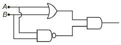
1. NAND gate
2. XOR gate
3. OR gate
4. NOR gate
लॉजिक गेट का निम्नलिखित विन्यास किसके समतुल्य है?

1. NAND गेट
2. XOR गेट
3. OR गेट
4. NOR गेट
© 2025 GoodEd Technologies Pvt. Ltd.